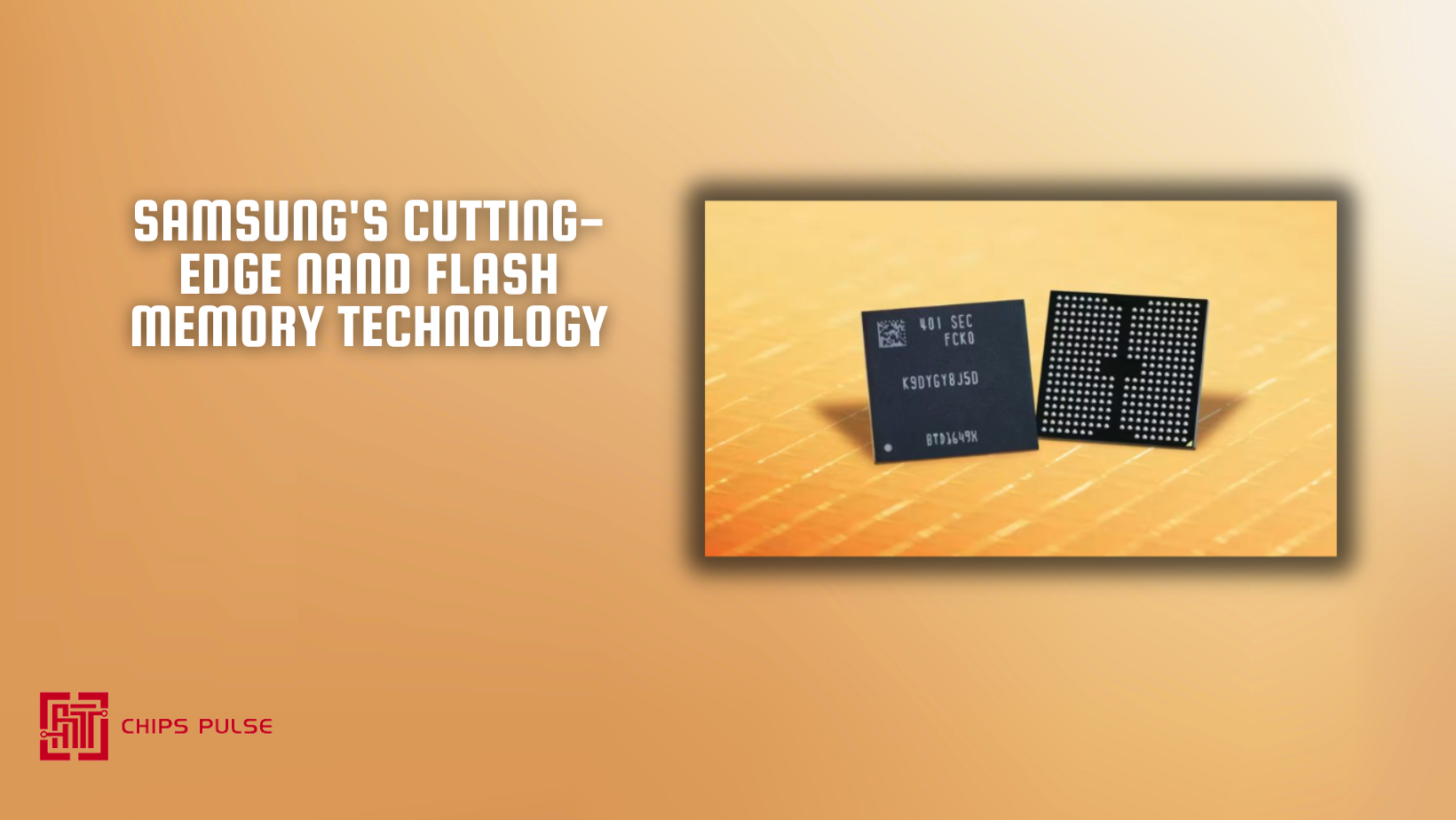
Samsung is once again pushing the boundaries of NAND flash memory technology with its 9th generation, 286-layer, 1Tbit TLC NAND flash memory, poised to revolutionize data storage capabilities. Not content with resting on their laurels, Samsung has announced plans for an even more impressive 10th generation with a staggering 400 layers.
Compared to its predecessor, the 8th generation 236-layer memory, the 286-layer device boasts remarkable improvements across the board. With a 50% increase in bit density, data input and output speeds enhanced by 33%, and a notable 10% reduction in power consumption, Samsung's latest innovation sets a new standard for NAND flash memory performance.
Key innovations driving these advancements include cell interference avoidance and cell life extension technologies. Notably, the elimination of dummy channel holes has significantly reduced the planar area of the memory cells, optimizing space utilization and enhancing overall efficiency.
Samsung’s proprietary "channel hole etching" technology is another breakthrough, creating electron pathways by stacking mold layers. This innovation maximizes fabrication productivity by enabling simultaneous drilling of the highest cell layer count in a double-stack structure. As the number of cell layers increases, so does the necessity for more sophisticated etching techniques.
The 9th-generation V-NAND is equipped with the Toggle 5.1 interface, supporting increased data input/output speeds by up to 3.2 Gbps, a 33% improvement over previous generations. This enhancement ensures rapid data transfer rates, crucial for applications demanding high-speed processing and responsiveness.
With the upcoming 10th generation promising even more layers and advancements, Samsung continues to drive innovation in NAND flash memory technology. As data storage needs grow exponentially, Samsung's commitment to pushing the boundaries of what's possible ensures that the industry remains at the forefront of storage capabilities.


Deutsch
USD $


.jpg)


